KiCAD Elecrow PCB service
Table of Contents
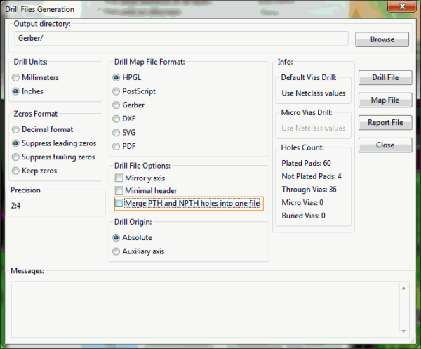
For the PCB service from Elecrow, following KiCAD have proven settings.
AGML battery charger
AGML battery charger
Verschiedene Designparameter und Notizen:
Design
Board Outline: 0.1mm
Via (0.3mm untented): Drill 0.3mm, Size 0.7mm, Soldermask clearance -0.1mm
Plane: 32 Segments/360Grad, Minimum 0.2mm, Clearance 0.2mm
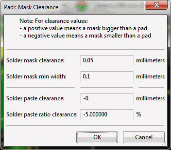
Pad Mask Clearance
Solder paste ratio clearance:-10%
Texts and Drawings
Copper Text Width: 0.15mm
Graphic segment width: 0.2mm
Text Size H/V: 0.8mm (0.6mm Minimum)
Text Module Width: 0.15mm
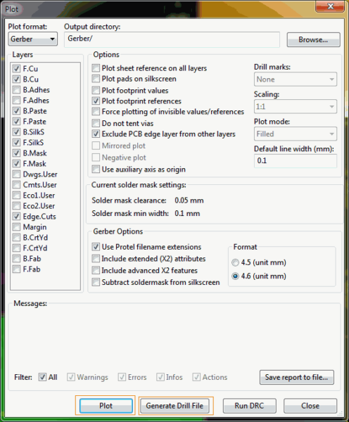
Plot
„Do not tent VIAs“
„Exclude PCB edge layer from other layers“


